SALD atomic coatings have the capacity to revolutionize numerous industrial manufacturing processes and therefore entire sectors of industry. These include solar panels and batteries for electric mobility and smartphones, as well as new kinds of textiles for fashion and medical products and packaging for the food sector and consumer goods. The Dutch company Sald B.V. has developed this technology in cooperation with several renowned European research institutes.
Further development of ALD
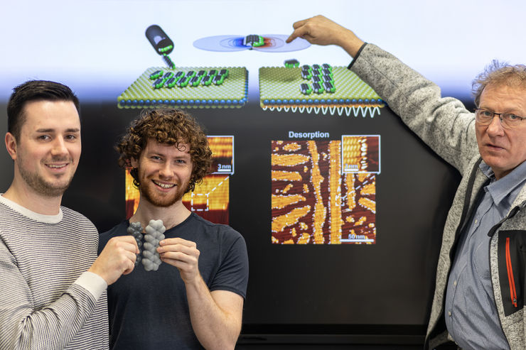
Spatial Atomic Layer Deposition (SALD) was first used industrially around ten years ago to produce an ultra-thin aluminum oxide film as a neutralization layer in solar cells, thus increasing the efficiency of the energy generation process. This first commercial application took place at Sald’s sister company Solaytec and had great success in the solar industry. The company Sald B.V. was spun off from this with the aim of further advancing the use of the technology and to take it to market maturity in other sectors. In this process, materials are coated with atom-thin layers, ultimately creating a three-dimensional structure that is not even a nanometer thick, even when nine layers are applied sequentially. According to the company, no other industrial process is currently able to achieve such uniformity, density, and structural conformity of the layers on structural surfaces. SALD is a further development of Atomic Layer Deposition (ALD), which has already been in use for a long time, for example in the semiconductor sector. Today’s highly integrated chips, such as those with 11.8 billion circuits in Apple’s latest A14 processor with a structure width of 5 nm, would be impossible without the previous ALD process. As the adjective “spatial” suggests, SALD adds a new dimension to this.
Three-dimensional atomic nanocoatings
In the SALD process, atomic layer coatings are applied three-dimensionally to surfaces. Each layer is as thin as an individual atom, and these layers envelop the surface as they are applied sequentially. A single layer is around 1.1 Å (1 ångström = 0.1 nm) thick, which is equivalent to 0.00011 μm. A particularly interesting feature is the possibility to mix the layers: different materials can be applied with each separate layer, thus allowing a chemical reaction to take place with the substance applied previously. For example, the surface materials can be metals, oxides, nitrides, sulfides, fluorides, or other substances. The respective chemical reaction therefore changes the functionality of the overall surface.
The complete article was published in IST 02/2021.
Autor(en): Erik Kremers, SALD B.V. Eindhoven, Netherlands